MPI TS2000 automated wafer probe systems
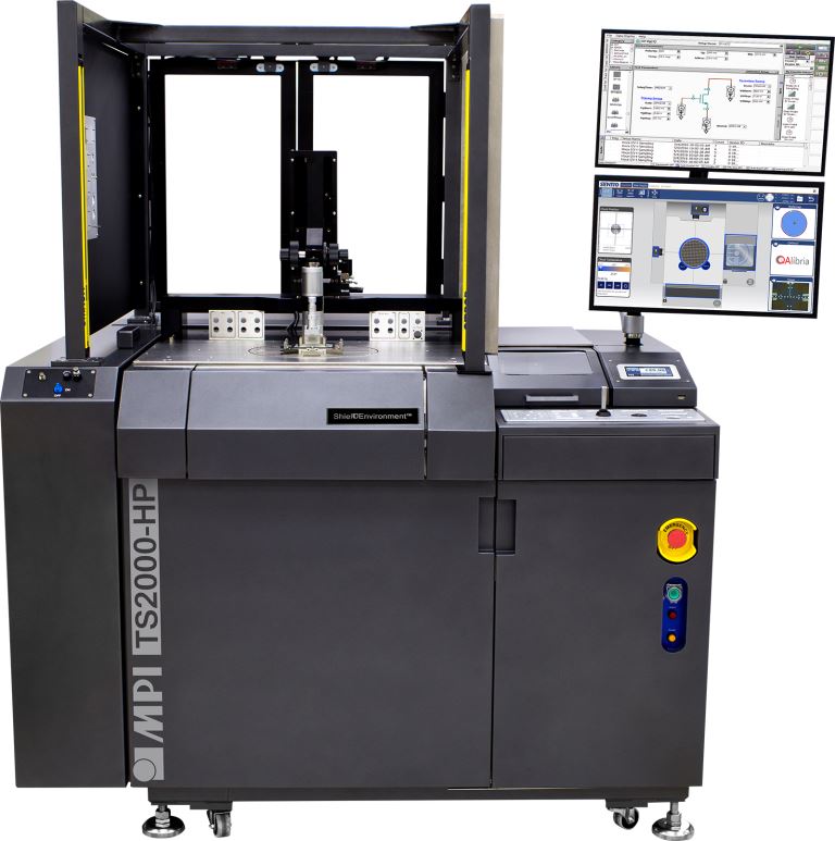
MPI TS2000-SE automated wafer probe systems with ShielDEnvironment
MPI TS2500-RF automated wafer probe systems for HF applications
MPI TS3000 automated wafer probe systems
MPI TS3000-SE automated wafer probe systems with ShielDEnvironment
Datasheets, Downloads, and Manuals
- MPI TS200 Datenblatt englisch
- MPI TS200-SE Datenblatt englisch
- MPI TS2500-RF englisch
- MPI TS3000-englisch
- MPI TS3000-SE englisch