TS 50 wafer probe system designed for IC Engineering, Single Die probing and academic use in DC/CV and RF measurement applications. Wafers up to 50mm
TS 150 engineering wafer probe system is a cost effective yet highly accurate manual probe system designed for precision analysis of substrates and 150mm wafers
TS 150-HP engineering wafer probe system is a cost effective yet highly accurate manual probe system designed for precision analysis of substrates and 150 mm wafers
TS 150-THZ engineering wafer probe system is a cost effective yet highly accurate manual probe system designed for precision analysis of substrates and 150 mm wafers. The TS150-THZ may be configured to support a wide variety of RF and millimeter wave (mmW) applications such as broadband up to 110 GHz, banded wave guide, sub-THz, load-pull and RF noise
TS 200 engineering wafer probe system is a cost effective yet highly accurate manual probe system designed for precision analysis of substrates and 200 mm wafers
TS 200-SE wafer probe systems with ShieldEnvironment™ provide maximum EMI shielding and allow low noise device on-wafer measurements for wide verity of applications
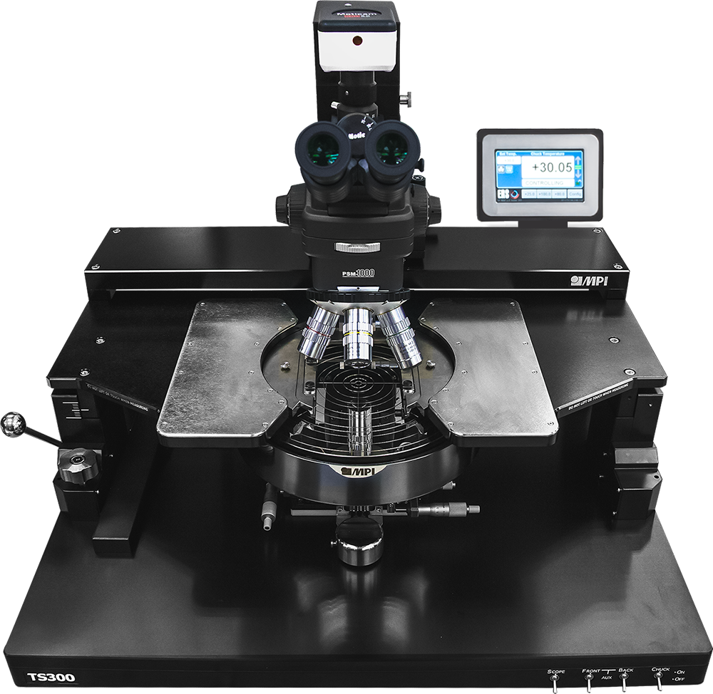
TS 300 engineering wafer probe system is a cost effective yet highly accurate manual probe system designed for precision analysis of substrates and 300 mm wafers
TS 300-SE is designed to ensure advanced EMI/RFI/light-tight shielding, ultra-low noise, low leakage measurement capabilities on 300 mm wafer in a temperature range from -60 to +300°C
Datasheets, Downloads, and Manuals
- MPI-TS50 Datenblatt englisch
- MPI TS150 Datenblatt englisch
- MPI TS150-HP Datenblatt englisch
- MPI TS150-THZ Datenblatt englisch
- MPI TS200 Datenblatt englisch
- MPI TS200-SE Datenblatt englisch
- MPI TS300 Datenblatt englisch
- MPI TS300-SE Datenblatt englisch